New Delhi, Nov 22
With rapid infrastructure development, a strong pipeline of global investors and India’s most comprehensive semiconductor manufacturing ecosystem, Dholera in Gujarat is emerging as a major driver of India’s industrial transformation and a preferred hub for next-generation industries, according to Commerce Ministry.
Dholera Industrial City has emerged as a key destination for strategic international engagements exploring opportunities in advanced manufacturing, semiconductors and smart industrial ecosystems.
According to the ministry, Japanese companies continue to expand their presence across NICDC industrial cities, reflecting strong confidence in India’s manufacturing ecosystem.
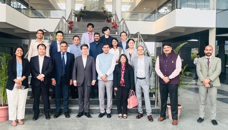
Nobumitsu Hayashi, Governor of Japan Bank for International Cooperation (JBIC), led a delegation to the National Industrial Corridor Development Corporation (NICDC) flagship industrial park, Dholera Special Investment Region (Dholera SIR) to review the progress of India’s first and emerging Semicon City and assess the fast-advancing greenfield and ‘Plug-and-Play’ industrial infrastructure ecosystem.
Hayashi appreciated the world-class planning, infrastructure readiness and strong governance framework of Dholera SIR. He expressed confidence in India’s semiconductor growth story and noted the rapid progress of the Tata Electronics Semiconductor Fabrication Facility.
He stated that Dholera’s integrated systems, scalable utilities and future-ready infrastructure make it a globally competitive destination for advanced electronics and semiconductor investments.
At the Tata Electronics Semiconductor Fabrication Facility in Dholera SIR, the delegation held discussions with Tata Group leadership and reviewed the 163-acre semiconductor fabrication plant being developed with an investment of Rs 91,000 crore in partnership with Powerchip Semiconductor Manufacturing Corporation (PSMC), Taiwan.
The facility, India’s first commercial semiconductor fabrication plant, will commence production in 2027, manufacturing 50,000 wafers per month across 110 nm to 28 nm nodes and generating more than 20,000 high-skilled jobs.
Hayashi expressed optimism that the project would strengthen India–Japan technological collaboration and contribute to global semiconductor value chains.
The visit comes at a time when India is witnessing unprecedented momentum in semiconductor manufacturing, with Dholera positioned at the forefront as the country’s most ambitious greenfield smart industrial city.
Recently, Ambassador of Japan to India and Bhutan, Ono Keiichi, led a 70-member Japanese business delegation representing sectors such as semiconductors, electronics, machinery, infrastructure, logistics and financial services.
Over the past year, Dholera has hosted delegations from JBIC, the Japan Chamber of Commerce, the Japan External Trade Organization (JETRO), JICA, leading Japanese corporations and global investors, according to the ministry.